Getting started:
Download the files for Lab 6 first.
Part I: FSM
Exercise 1: FSMs to Digital Logic
In this exercise, you need to translate a FSM into a digital logic circuit. FSM's keep track of inputs given, moves between states based on these inputs, and outputs something everytime something is input. We use a register to store the state of the FSM we're currently in, and combinational logic to map FSM input & current register state to FSM output & next register state.
ACTION ITEM:
Load the given starter file ex1.circ into Logisim. Modify this circuit's subcircuits StateBitZero and StateBitOne to implement this Moore FSM: Detecting 010 pattern in a bit sequence(use overlapping). Show this completed circuit to your TA (remember to save!)
-
Note that the FSM is implemented by the following diagram (the four state names
00,01,10,11are just names written in binary - they have no direct relationship with the actual zeros and ones of the FSM input/output). Take some time to understand how this diagram implements the FSM: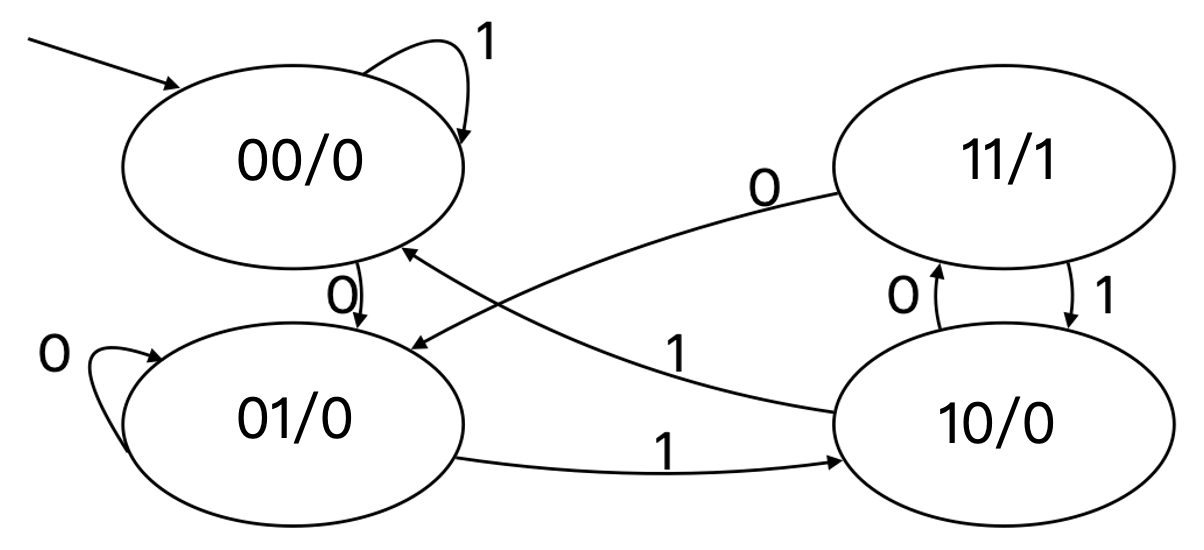
-
Observe that the following is a truth table for the FSM (convince yourself of this):
st1 st0 input next st1 next st0 output 0 0 0 0 1 0 0 0 1 0 0 0 0 1 0 0 1 0 0 1 1 1 0 0 1 0 0 1 1 0 1 0 1 0 0 0 1 1 0 0 1 1 1 1 1 1 0 1 -
We've provided you with a starter Logisim circuit to start out in
ex1.circ. -
Note that the top level of the circuit looks almost exactly the same as our previous adder circuit, but now there's a
FSMLogicblock instead of an adder block.FSMLogicis the combinational logic block for this FSM. We have handled the output bit for you. You should complete the circuit by completing theStateBitOneandStateBitZerosubcircuits, which produces the next state bits.
Check-off
StateBitZero circuit & StateBitOne circuit to your TA and demonstrate that they behave correctly.
Part II: Introduction to RV32 CPU
Exeicise 2: Program Counter
In the RV32I CPU, the Program Counter (PC) is a core component responsible for tracking the address of instructions. Below is a detailed description of the PC's functionality, input, and output ports:
Functionality:
- Instruction Address Tracking: The PC holds the address of the next instruction to be executed. In most cases, the PC increments by 4 (since RV32I instructions are 32 bits wide, or 4 bytes) each clock cycle, pointing to the next sequential instruction.
- Jump and Branch Support: When a jump or branch instruction is encountered, the PC is updated to the new target address instead of simply incrementing.
- Exception and Interrupt Handling: In the event of an exception or interrupt, the PC is updated to the entry address of the exception handler or interrupt service routine.
Input Ports:
- Clock Signal (clk): The clock signal synchronizes the update of the PC. On each clock cycle's rising edge, the PC updates its value based on control signals.
- Reset Signal (reset): The reset signal initializes the PC to its default value (typically 0x00000000).
- PC Update Signal (pc_update): This signal indicates whether the PC needs to be updated. It serves as a control signal for a multiplexer, selecting the next value for the PC (e.g., sequential increment, jump address, branch address, etc.).
- New Address Input (new_addr): When the PC needs to be updated to a new address (e.g., during a jump or branch), the target address is provided through this input port.
Output Ports:
- Current Address Output (current_addr): The PC outputs the currently held instruction address, which is sent to the instruction memory to fetch the next instruction to be executed.
ACTION ITEM:
Load the given starter file ex2.circ into Logisim and implement a PC circuit. Show this completed circuit to your TA (remember to save!)
Details:
In this lab, All instructions are a fixed 32 bits in length, meaning that instructions must be aligned on a 4-byte boundary in memory.
But sometimes, An instruction-address-misaligned exception is generated on a taken branch or unconditional jump if the target address is not 4-byte aligned.
In this case, it needs to be automatically rounded down to 4-byte alignment. For example, if the target address is 0x000000A3, you need to align it to 0x000000A0.
Check-off
- The architecture of your circuit;
- How your circuit handles the misaligned address.