Download the files for Lab 5 first.
Something you must know before you start:.jar file we have provided (Version 3.8.0) to avoid compatibility issues. Windows, Ubuntu and macOS systems can all run it.Command/Control + S shortcut key allows for quick saving..jar file with the left mouse button. If you launched Logisim from the command line, please keep the terminal open while it is running, otherwise the program will immediately exit.
$ java -jar logisim-evolution.jarIn this part of the lab, we will create an
AND gate circuit together to help us get started quickly. Please pay attention to the zoom and grid functions located at the bottom left corner of the program, which will facilitate your wiring process during larger circuit designs.
 Start by clicking the
 AND gate button. This will cause the shadow of an AND gate to follow your cursor around. Click once within the main schematic window to place an AND gate.
 Click the
 Input Pin button. Now, place two input pins somewhere to the left of your AND gate.
 Click the
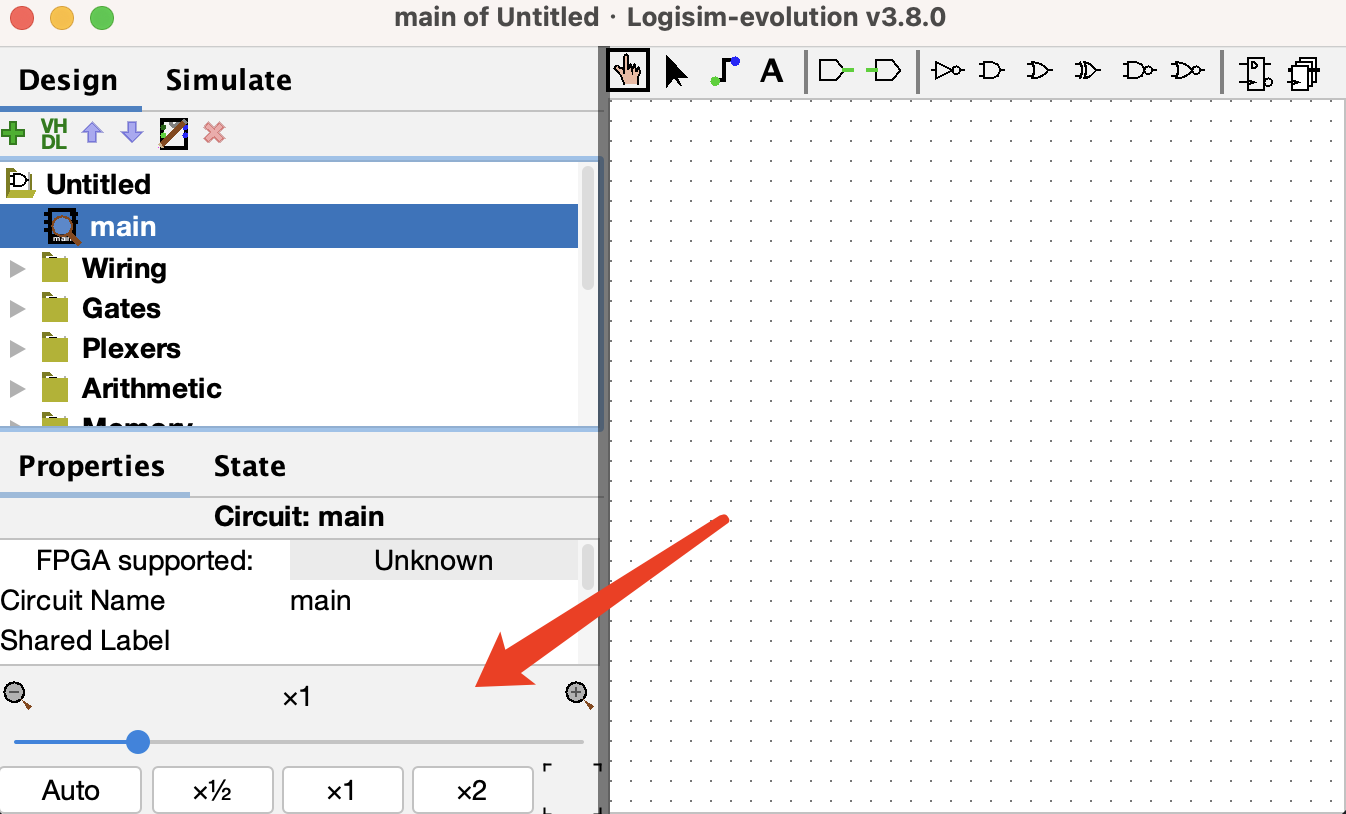
 Output Pin button. Then place an output pin somewhere to the right of your AND gate. Your schematic should look something like this at this point:
 Click the
 Select tool button. Click and drag to connect the input pins to the left side of the AND gate. This will take several steps, as you can only draw vertical and horizontal wires. Just draw a wire horizontally, release the mouse button, then click and drag starting from the end of the wire to continue vertically. You can attach the wire to any pin on the AND gate on the left side. Repeat the same procedure to connect the output of the AND Gate (right side) to the output pin. Double-click these three pins to name them labels. After completing these steps your schematic should look roughly like this:

 Click the
 Poke tool and try clicking on the input pins in your schematic. Observe what happens. Does this match with what you think an AND Gate should do? Note that poking the wires themselves tells you the current value on that wire; this will be very useful later when you build more complex circuits.
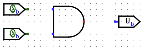
ex1.circ. Click Simulate -> Test Vector... and load vector selecting the testvector_ex1.txt file from the lab5_starter folder. If everything goes well, you should see that all four test vectors passed.
IMPORTANT NOTE: Logisim Evolution guidlines say you cannot name a subcircuit after a keyword (e.g. NAND), also circuit names must start with "A-Za-z", so no numbers.
Open up the Exercise 2 schematic (File -> Open -> ex2.circ).
Open up the NAND1 empty subcircuit by double clicking on the name NAND1 in the circuit selector in the left menu. (note the 1 at the end; because there is a component called NAND, we cannot call it NAND).
In the new schematic window that you see create a simple NAND circuit with the 2 input pins on the left side and the output pin on the right side. Do this without using the built-in NAND gate from the Gates folder (i.e. only use the AND, OR, and NOT gates provided next to the selection tool icon). You can change the labels for the inputs and output by selecting the input/output using the select tool and changing the property Label in the bottom left of the window.
Repeat these steps to create several more subcircuits: NOR, XOR, 2-to-1 MUX, 4-to-1 MUX and HALF ADDER in the given skeletons. Please do not change the names of the subcircuits or create new ones; do you work in the respectively named circuit or else the autograder will not work properly. Do not use any built-in gates other than AND, OR, and NOT. Once you've built a subcircuit, you may (and are encouraged to) use it to build others. You can do this by clicking and placing your created subcircuit like you would any other component.
Note: for the 4-to-1 MUX, Sel1 and Sel2 correspond to the 1st and 2nd bits of the 2-bit selector, respectively.
Build your 4-to-1 MUX according to the following rule in this lab:
Sel1: 0, Sel2: 0 -> Select A
Sel1: 1, Sel2: 0 -> Select B
Sel1: 0, Sel2: 1 -> Select C
Sel1: 1, Sel2: 1 -> Select D
Hint: Try writing a truth table. You might also find the lecture slides useful for a refresher on how to build these. You may want to consider using some of your custom subcircuits when designing the others.
NAND, NOR, XOR, 2-to-1 MUX, 4-to-1 MUX and HALF ADDER) to your TA.Let's implement a circuit that increments a value ad infinitum. The difference between this circuit and the circuits you've built for lab so far is that it will store this value in the state of a register.
The following steps will show you how to add registers to your circuit. Complete the steps and show the final circuit to your TA (remember to save!):
Open up the Exercise 3 schematic (File -> Open -> ex3.circ) and go to the empty AddMachine circuit.
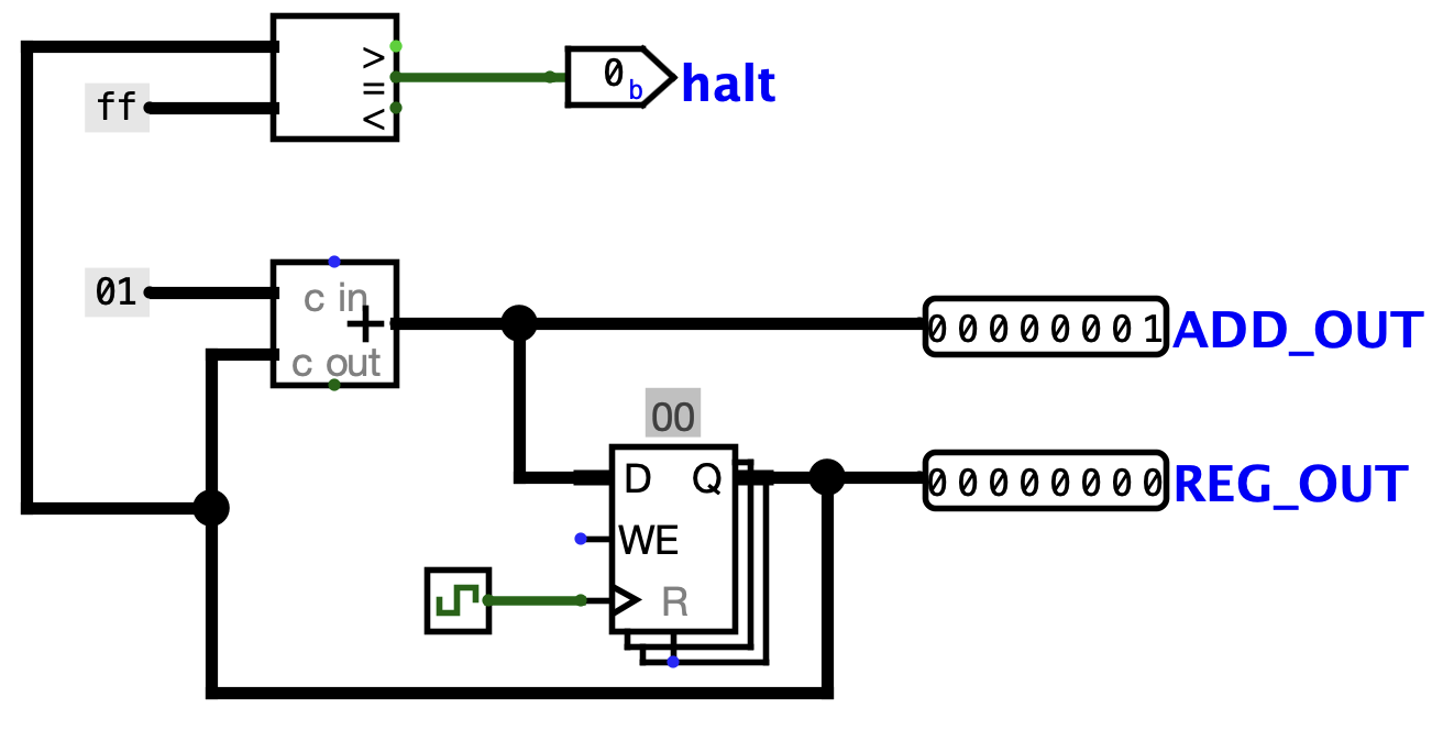
Select the Adder subcircuit from the Arithmetic library and place the Adder into your AddMachine subcircuit.
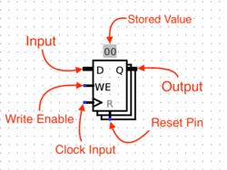
Select the register from the Memory folder and place one register into your subcircuit. Below is an image diagraming the parts of a register.
Connect a clock to your register. You can find the clock circuit element in the Wiring folder in the circuit browser.
Adder to the input of the register, and the output of the register to the input of the Adder.
Adder with the Selection tool, you will notice that there is a Data Bit Width property in the bottom left field of the window. This value determines the number of bits each input and output the Adder has. Change this field to 8 and the "Incompatible widths" error should be resolved.Wire an 8-bit constant 1 to the second input of the Adder. You can find the Constant circuit element in the Wiring library.
Connect the two output pins to your circuit so that you may monitor what comes out of the Adder and the register. The output of the Adder should be connected to ADD_OUT and the output of the register to REG_OUT.
Select the Comparator subcircuit from the Arithmetic library and place the Comparator into your AddMachine subcircuit. The first input of the Comparator should be connected to REG_OUT. Wire an 8-bit constant 255 to the second input of the Comparator.
Create an output pin at the right of the Comparator and name its label as halt. Connect the second output of the Comparator to the halt. It is used as a flag indicating the end of the simulation. Thus, by the end, your circuit should look like as follows:
Now start running your circuit by going to Simulate->Ticks Enabled (or Command/Control + K). Your circuit should now be outputting a counter in binary form.
If you want to run your circuit faster, you can change the tick frequency in Simulate->Tick Frequency.
AddMachine circuit to your TA.In this part of lab, we're ready to do something really cool: translate a FSM into a digital logic circuit. FSM's keep track of inputs given, moves between states based on these inputs, and outputs something everytime something is input. We use a register to store the state of the FSM we're currently in, and combinational logic to map FSM input & current register state to FSM output & next register state.
Load the given starter file ex4.circ into Logisim. Modify this circuit's subcircuits StateBitZero and StateBitOne to implement this Moore FSM: Detecting 010 pattern in a bit sequence(use overlapping). Show this completed circuit to your TA (remember to save!)
Note that the FSM is implemented by the following diagram (the four state names 00, 01, 10, 11 are just names written in binary - they have no direct relationship with the actual zeros and ones of the FSM input/output). Take some time to understand how this diagram implements the FSM:
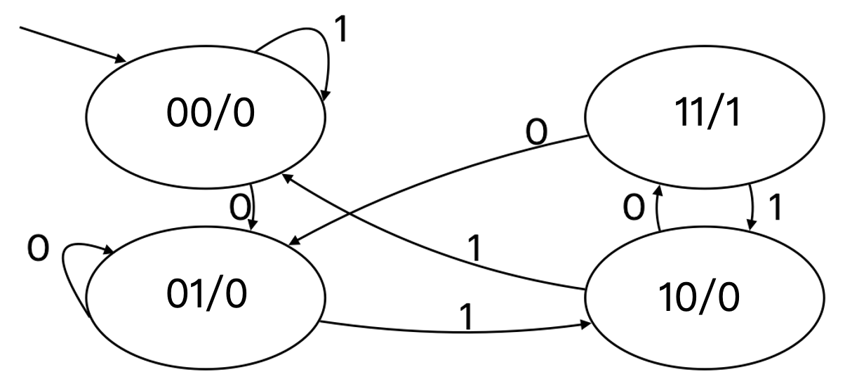
Observe that the following is a truth table for the FSM (convince yourself of this):
| st1 | st0 | input | next st1 | next st0 | output |
|---|---|---|---|---|---|
| 0 | 0 | 0 | 0 | 1 | 0 |
| 0 | 0 | 1 | 0 | 0 | 0 |
| 0 | 1 | 0 | 0 | 1 | 0 |
| 0 | 1 | 1 | 1 | 0 | 0 |
| 1 | 0 | 0 | 1 | 1 | 0 |
| 1 | 0 | 1 | 0 | 0 | 0 |
| 1 | 1 | 0 | 0 | 1 | 1 |
| 1 | 1 | 1 | 1 | 0 | 1 |
We've provided you with a starter Logisim circuit to start out in ex4.circ.
Note that the top level of the circuit looks almost exactly the same as our previous adder circuit, but now there's a FSMLogic block instead of an adder block. FSMLogic is the combinational logic block for this FSM. We have handled the output bit for you. You should complete the circuit by completing the StateBitOne and StateBitZero subcircuits, which produces the next state bits.
StateBitZero circuit & StateBitOne circuit to your TA and demonstrate that they behave correctly.
To test, run the testing script test.sh. Since Logisim will be running in one terminal window already, make sure to open up a new window to run the testing script. This script will copy your circuits into a testing harness, run your circuits on different inputs, and compare your results to ours. Therefore, please do not touch anything in the testing folder unless a TA instructs you to do so. However, you are more than welcome to check out the circuitry involved in testing your code as you will encounter it again when working on Project 2.